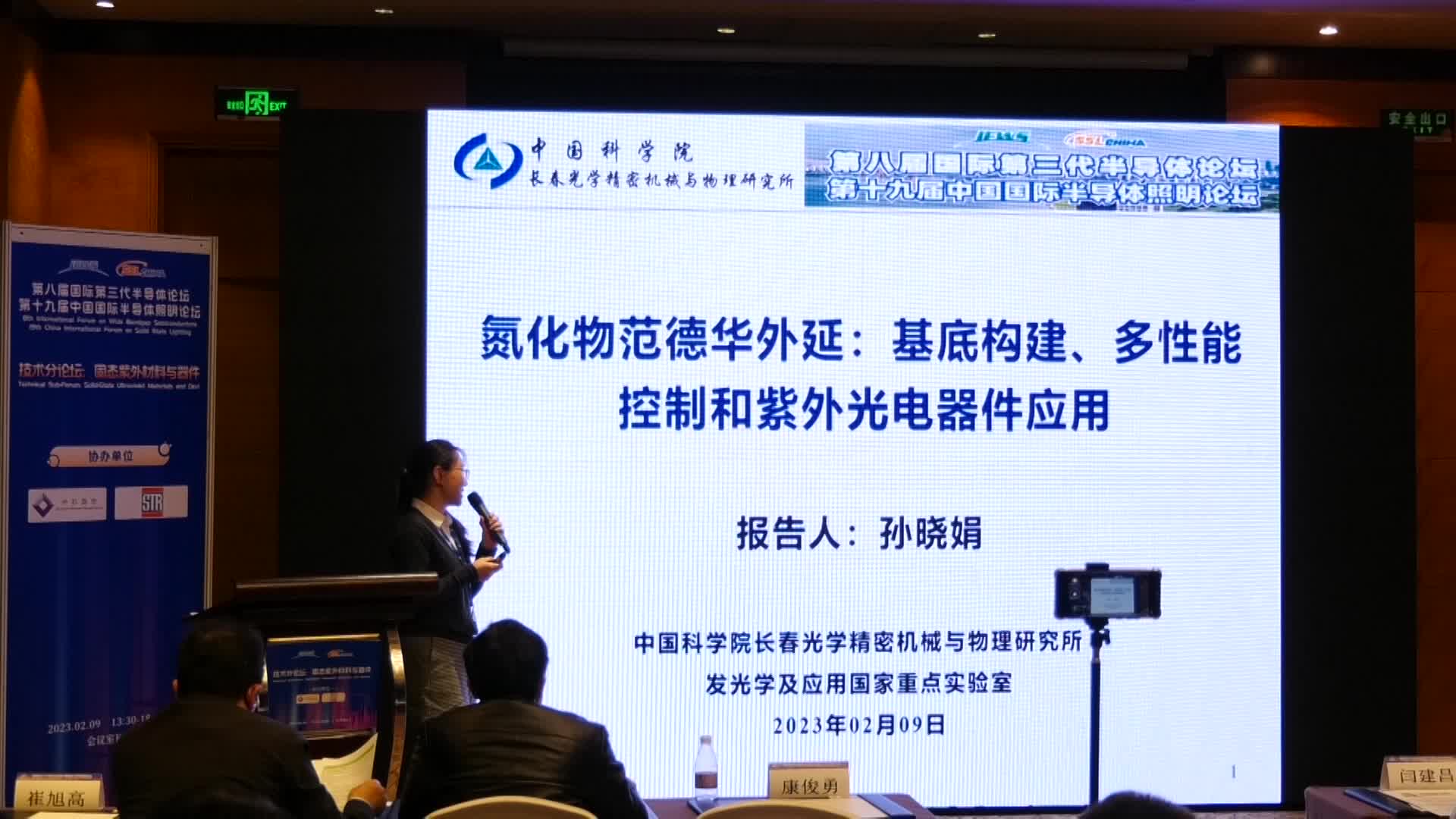
亚洲日韩久久|国偷自产一区二区三区蜜臀国|国产一区二区日韩|99热这里只亚洲无码,无码

  • 北京大學理學部副主任
    基于大失配外延的氮化物第三代半導體材料與器件Nitride Semiconductor Materials and Devices Based on Large Mismatch Epitaxy沈波北京大學理學部副主任、特聘教授SHEN Bo Deputy Deanand Distinguished Professorof Facultyof Science, Peking University
    322700
    IFWS2025-01-09 15:42
  • 普興電子市場總監(jiān)張國
    大直徑碳化硅外延市場發(fā)展與挑戰(zhàn)Development and Challenges of Large Diameter Silicon Carbide Epitaxial張國良河北普興電子科技股份有限公司市場總監(jiān)ZHANG GuoliangMarketing Director of Hebei Pushing Electronic Technology Co., LTD
    55500
    IFWS2025-01-09 15:04
  • AIXTRON中國總經(jīng)理方
    化合物半導體外延大規(guī)模量產(chǎn)解決方案High Volume Manufacturing of Compound Semiconductors Epitaxy方子文AIXTRON中國總經(jīng)理FANG ZiwenGM of AIXTRON China
    56000
    IFWS2025-01-09 14:59
  • 中科重儀半導體聯(lián)合創(chuàng)
    GaN基光電材料外延與MOCVD反應腔結(jié)構關聯(lián)性研究Research on the Correlation Between GaN-based Optoelectronic Material Epitaxy and MOCVD Reactor Chamber Structure姚威振中國科學院半導體研究所副研究員、中科重儀半導體聯(lián)合創(chuàng)始人YAO WeizhenAssociate Professor of Institute of Semiconductors, Chinese Academy of Sciences, Co-founder of CASInstruments Semiconductor Co., Ltd.
    21200
    IFWS2025-01-09 14:42
  • 中科院蘇州納米所研究
    硅襯底GaN基光電材料外延生長Epitaxial Growth of GaN Based Photoelectric Materials on Silicon Substrate孫錢中國科學院蘇州納米技術與納米仿生研究所研究員SUN QianProfessorof Suzhou Institute of Nano-Tech and Nano-Bionics (SINANO), Chinese Academy of Sciences
    55400
    IFWS2025-01-09 14:41
  • 南京大學劉歡:等離子
    等離子體輔助分子束外延生長AlN薄膜AlN epilayers grown by plasma assisted molecular beam epitaxy劉歡南京大學LIU HuanNanjing University
    34400
    IFWS2025-01-09 14:40
  • 辰華半導體郭炳磊:用
    用于氮化鎵異質(zhì)外延的高溫PVD氮化鋁緩沖層技術High Temperature PVD AlN e Buffer Layer Technology for GaN Heteroepitaxy
    21100
    IFWS2025-01-09 14:28
  • 中電科第十三所高級工
    6英寸復合襯底上厚GaN外延生長研究Growth of Thick GaN Epilayers on 150mm Engineered Substrate韓穎中國電子科技集團第十三所高級工程師HAN YingSenior Engineer of Hebei Semiconductor Research Institute
    32400
    IFWS2025-01-09 14:27
  • 思體爾總經(jīng)理LAMBRINA
    基于量產(chǎn)的氮化鎵基光電子及功率器件的外延建模Modeling of Production-scale Epitaxy for Optical and Power GaN-based Devices LAMBRINAKIMARIIA蘇州思體爾軟件科技有限公司總經(jīng)理LAMBRINAKI MARIIAGeneral Manager of Suzhou STR Software CO.,Ltd.
    121100
    IFWS2025-01-09 14:20
  • 鎵和半導體李山:氧化
    氧化鎵PECVD外延生長及光電信息感知器件研究Research on PECVD Epitaxial Growth of Gallium Oxide and the Photoelectric Information Sensing Devices李山南京郵電大學副教授、蘇州鎵和半導體研發(fā)總監(jiān)LI ShanAssociate Professor, Nanjing University of Posts and Telecommunications, RD director of Suzhou GAO Semiconductor Co. Ltd.
    55300
    IFWS2025-01-09 13:53
  • 中科院長春光機所研究
    氮化物的范德華外延:基底結(jié)構、多性能控制和紫外光電器件應用Van der Waals Epitaxy of Nitrides: Substrate Construction, Multi-Properties Control and Ultraviolet Optoelectronic Device Application孫曉娟中科院長春光機所研究員SUN XiaojuanProfessor of Changchun Institute of Optics, Fine Mechanics and Physics, Chinese Academy of Sciences
    118700
    guansheng2023-05-19 14:58
  • 西安電子科技大學張金
    MPCVD法金剛石同質(zhì)外延生長及MOS器件技術Homogeneous epitaxial diamond growth by MPCVD and its MOS device technology張金風西安電子科技大學教授ZHANG JinfengProfessor of Xidian University
    159600
    guansheng2023-05-19 14:40
  • 湖北大學何云斌教授:
    MgO(100)上生長柱狀納米晶b-Ga2O3外延薄膜及其高靈敏度日盲探測器研究Columnar-nanodomained epitaxial b-Ga2O3 thin films on MgO(100) for solar-blind photodetectors with exceedingly high sensitivity何云斌湖北大學教授HE YunbinProfessor of Hubei University
    113500
    guansheng2023-05-19 14:23
  • 沙特阿卜杜拉國王科技
    面向柔性和垂直電子器件的外延氧化鎵薄膜Epitaxial Ga2O3 thin film membrane for flexible and vertical electronics李曉航沙特阿卜杜拉國王科技大學副教授(陸義代講)LI XiaohangAssociate Professor at King Abdullah University of ScienceTechnology
    98800
    guansheng2023-05-19 14:15
  • 江蘇第三代半導體研究
    高性能GaN-on-GaN材料與器件的外延生長High output power and bandwidth of c-plane GaN-on-GaN micro-LED for high-speed visible light communication王國斌江蘇第三代半導體研究院研發(fā)部負責人WANG GuobinSenior Project ManagerHead of RD Dept of Jiangsu Institute of Advanced Semiconductors
    129000
    guansheng2023-05-19 08:56
  • 武漢大學工業(yè)科學研究
    無損表征氮化鎵外延熱物性的瞬態(tài)熱反射技術Transient thermoreflectance technique for non-invasively characterizing the thermal properties of GaN epitaxial wafer袁超武漢大學工業(yè)科學研究院研究員YUAN ChaoProfessor of The Institute of Technological Sciences, Wuhan University
    121200
    guansheng2023-05-19 08:53
  • 北京大學副教授許福軍
    AlGaN基低維量子結(jié)構外延和電導率調(diào)控研究Study on the epitaxy and conductivity regulation of AlGaN based low dimensional quantum structures許福軍北京大學物理學院副教授Xu Fujun - Associate Professor, Peking University
    121900
    guansheng2023-05-19 08:51
  • 奧趨光電CTO王琦琨:P
    PVT法同質(zhì)外延AlN生長和p型摻雜面臨的挑戰(zhàn)Challenges on homoepitaxial AlN growth and p-type doping by the PVT method王琦琨奧趨光電技術(杭州)有限公司研發(fā)總監(jiān)(CTO)
    54500
    guansheng2023-05-19 08:43
  • 桑立雯:利用AlN傳導
    利用AlN傳導層在GaN襯底上外延生長金剛石薄膜及其熱傳輸特性Thermal dissipation from GaN to diamond with AlN conduction layer桑立雯日本國立物質(zhì)材料研究所獨立研究員SANG LiwenIndependent Scientist of National Institute for Materials Science (NIMS), Japan
    64600
    guansheng2023-05-19 08:42
  • 中國科學院半導體所研
    平片藍寶石襯底上高質(zhì)量AlN材料MOCVD外延生長High quality AlN growth on flat sapphire at relative low temperature by MOCVD趙德剛中國科學院半導體所研究員ZHAO DegangProfesor of Institute of Semiconductors, CAS
    70900
    guansheng2023-05-18 16:19
聯(lián)系客服 投訴反饋  頂部